3d dram admnd tsv differences
62 Using a Test Die to Test Passive Interposers at Wafer Sort Xilinx 63 Timing and Test Techniques for 24 Gbspin. Cannot accurately capture the faulty behavior of TSV open defects in 3D DRAM.
Tsv Vs Monolithic 3d
Our goal however is to encourage the research.

. Die size difference die thickness etc. To meet the performance. Based on SSD market price there are about 10 to 30 price difference.
Ad Complete 3D Design Solutions. AMD revealed at a recent high performance computing event that it is working on new designs that use 3D-stacked DRAM and SRAM on top of its. As CPU performance has continually enhanced by transistor scaling the demand in DRAM performance has been also increased.
Published March 17 2019. Therefore in order to expand lifespan of DRAM 3D DRAM must be required for the DRAM in short time. 3D Event Coverage Blogs Francoise in 3D.
Right- IBM embedded DRAM with Cu TSVs. Download scientific diagram TSV locations in 3D DRAM vs. AMD already stacks HBM2 memory next to its GPU die meaning it resides in the same package as the processor but the company plans to move to true 3D stacking in the near.
The Many Flavors of 3D DRAM. The integration of Via-middle TSV processes in DRAM technology with major. Oct 09 2013 By Francoise von Trapp 3D DRAM 3D NAND DBI DRAM HBM HMC Monolithic 3D.
61 Overview of Test Yield and Repair of 3D TSV DRAMProcessor Chips. Relying on its 12-layer 3D-TSV technology Samsung will offer the highest DRAM performance for applications that are data-intensive and extremely high-speed. A 3D packaging technology has been developed for DRAM using highly doped poly-Si TSVs 9.
TSV formation wafer thinning microbump fabrication and chip stacking are key processes for 3D chip stacking using TSV. Further as these architectures evolve and new 3D memory organizations emerge the specific differences may change. In addition as the coupling effects between aggressor TSVs and victim TSV vary with the op-eration of the.
In this paper the process steps of TSV formation. Also by increasing the number. Relying on its 12-layer 3D-TSV.
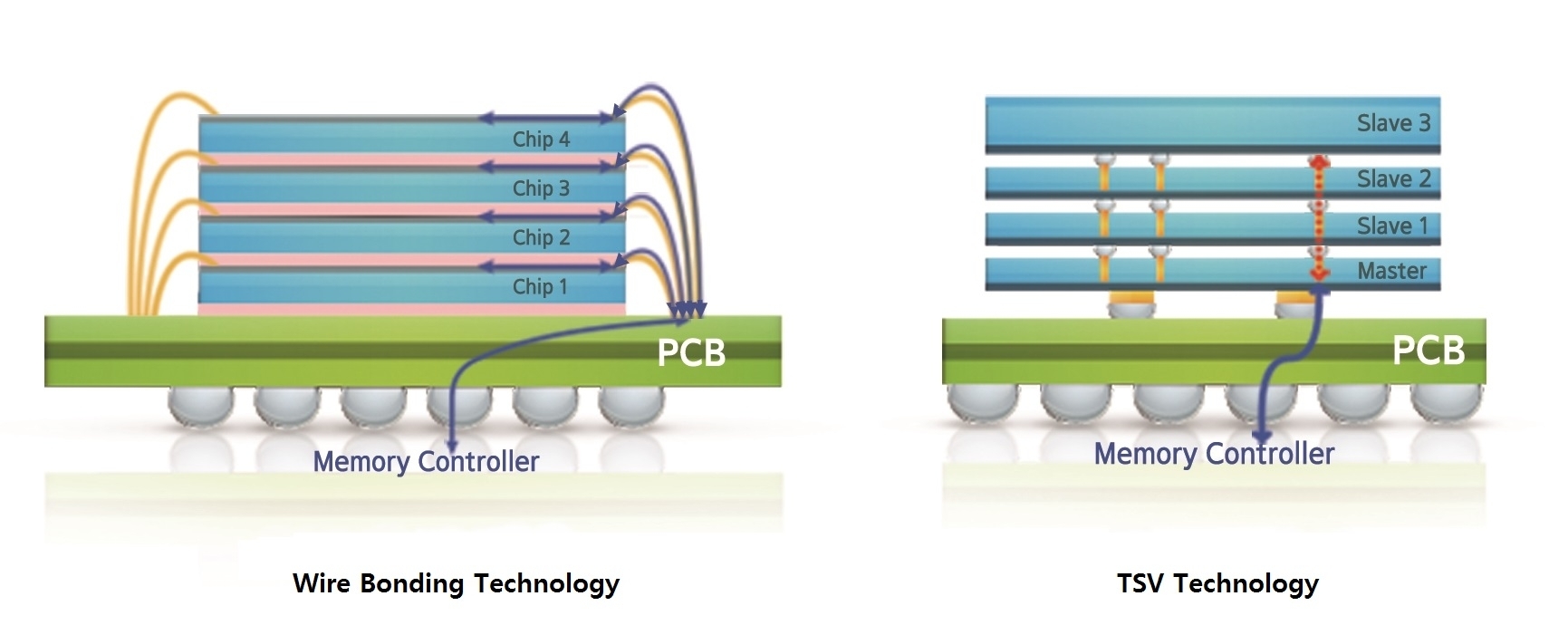
DRAM Dynamic Random Access Memory is among the most often employed architectures due to its cost-effectiveness as compared to SRAM Static Random-access. That is what Samsung is boasting off in its new DRAM technology that is able to stack 12 DRAM chips in the same space as 8 chips by ditching the traditional wire-bonding.
Samsung Electronics Develops Industry S First 12 Layer 3d Tsv Chip Packaging Technology Business Wire

Electronics Free Full Text Case Study On Integrated Architecture For In Memory And In Storage Computing Html

Hbm3 Big Impact On Chip Design
The Journey Of Dram Continues Semiwiki
3d Stacked Dram Example High Bandwidth Memory Consists Of Stacked Download Scientific Diagram

3d Layer Stacking Tsv Technologies Set To Refresh Memory

Stress Induced Performance Shifts In 3d Drams

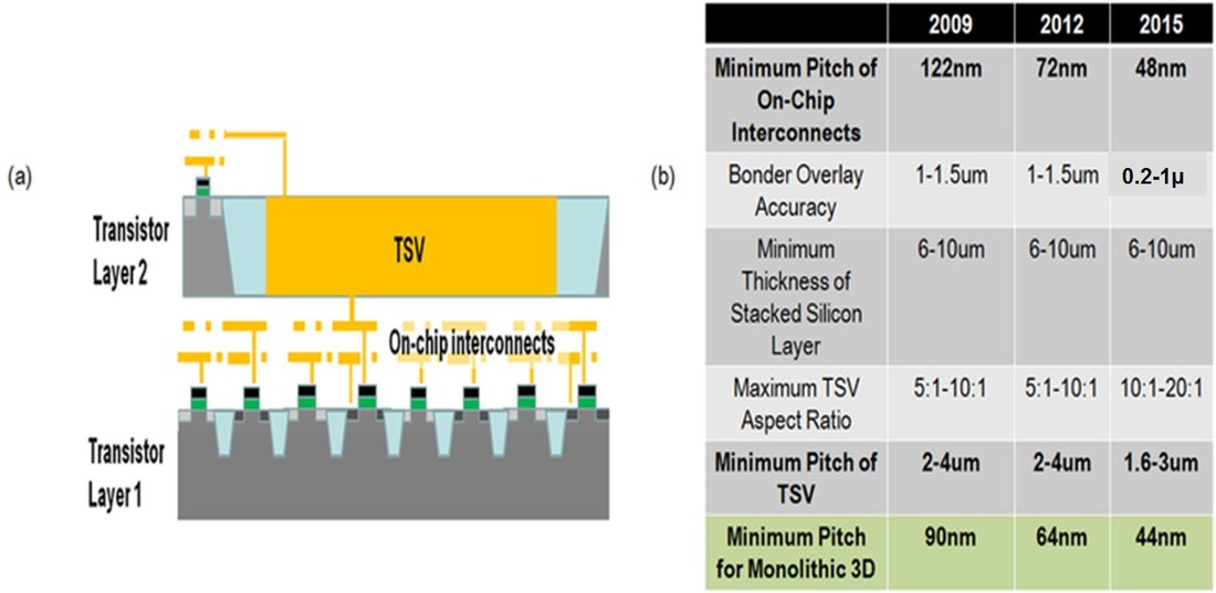
3d Tsv Roadmap Tsv Implementations Probably Evolve From Cmos Image Download Scientific Diagram

Putting 3d Integration To The Test 3d Incites

2d Planar Dram Architecture And 3d Dram Architectures With Different Download Scientific Diagram

2d Planar Dram Architecture And 3d Dram Architectures With Different Download Scientific Diagram

An Energy Efficient 3d Heterogeneous Main Memory Architecture For Mobile Devices

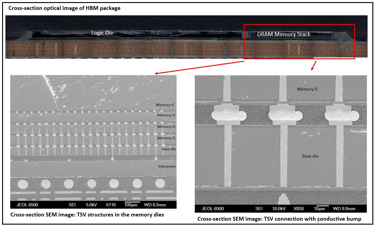
Samsung 3d Tsv Stacked Ddr4 Dram The First Analyzed Memory Product With Via Middle Tsv I Micronews

The History And Future Of Dram Architecture In Different Application Domains An Analysis Semiconductor Digest

3d Swift Memory Subsystem And Possible Applications A 3d Swift Download Scientific Diagram

Vertical Nand With And Without Tsv A Closer Look I Micronews

Various 3d Interconnect Approaches Between Logic And Memory Download Scientific Diagram

Tsv Locations In 3d Dram Vs Logic And Their Rdl Needs A Edge Download Scientific Diagram

Packaging Technology A Key To Next Generation Semiconductor Competitiveness How Far Has Sk Hynix Come Sk Hynix Newsroom